
Applied Materials opens new $5B chip research facility to accelerate collaborative semiconductor innovation
Semiconductor industry giant Applied Materials Inc. today opened the doors to its Equipment and Process Innovation and Commercialization Center, a massive new $5 billion facility in Silicon Valley that’s set to enable the next wave of breakthroughs in the commercial chipmaking industry.
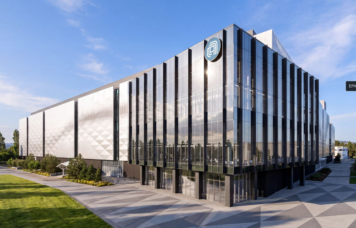
Applied Materials has opened a new $5 billion research facility in Silicon Valley, the Equipment and Process Innovation and Commercialization Center (EPIC), aimed at accelerating semiconductor innovation through collaborative R&D.
What happened
Applied Materials has launched the EPIC Center, a $5 billion research facility in Silicon Valley, to foster collaboration among semiconductor companies, academic institutions, and equipment providers. The center aims to accelerate the development of next-generation chip technologies by reducing R&D cycles and improving commercialization efficiency.
Why it matters
The EPIC Center addresses the growing demand for advanced semiconductors driven by AI and other high-performance computing needs. By shortening development timelines and enhancing collaboration, the facility helps meet the industry's urgent need for more efficient and powerful chip technologies.
- Collaborative R&D is critical for accelerating semiconductor innovation.
- The EPIC Center aims to cut development cycles by 30% through cross-industry partnerships.
- Advanced packaging and 3D architectures are key focus areas for next-gen chip development.
The bigger picture
The EPIC Center is expected to significantly reduce the time required to bring new semiconductor technologies to market, improve energy efficiency in computing, and enable advancements in AI, healthcare, and consumer electronics through collaborative innovation.
Applied Materials' EPIC Center represents a major step forward in semiconductor R&D, offering a collaborative platform to drive innovation and meet the rising demands of AI and high-performance computing.
Technical details
- 3D architectures
- advanced packaging techniques
- low-resistance wiring
- hybrid bonding
- atomic-scale materials development
- parallel R&D across industry partners
FAQ
What is the EPIC Center?
The EPIC Center is a $5 billion research facility opened by Applied Materials in Silicon Valley to accelerate semiconductor innovation through collaborative R&D with industry partners and academic institutions.
What are the main goals of the EPIC Center?
The main goals of the EPIC Center are to reduce semiconductor R&D cycles by 30%, improve energy efficiency, and enable faster commercialization of new chip technologies through cross-industry collaboration.
Who are the key partners involved in the EPIC Center?
The EPIC Center's founding partners include major chipmakers like TSMC, Intel, Samsung, and academic institutions such as Stanford University and UC Berkeley.
This summary and analysis were generated with AI from the original article and may contain errors. Read the original for the full story.
Read the full story
Originally published by SiliconANGLE on Oct 13, 2026.
Comments
Sign in to join the discussion.